TECH NEWS | New method may solve bottleneck of microelectronics: researchers
Researchers have developed a new method to fabricate silicon chips that can communicate with light and are no more expensive than current chip technology.

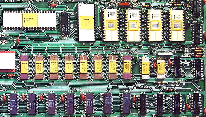
Electronic chip board
LOS ANGELES, CALIFORNIA — Researchers from Boston University, Massachusetts Institute of Technology, the University of California Berkeley and University of Colorado Boulder have developed a new method to fabricate silicon chips that can communicate with light and are no more expensive than current chip technology, according to the study, published in the latest issue of Nature.
The electrical signaling bottleneck between current microelectronic chips has left light communication as one of the only options left for further technological progress. The traditional method of data transfer-electrical wires-has a limit on how fast and how far it can transfer data. It also uses a lot of power and generates heat.
With the relentless demand for higher performance and lower power in electronics, these limits have been reached.
However, according to the new study, which is the culmination of a several-year-long project funded by the U.S. Defense Advanced Research Project Agency, the new microchip technology capable of optically transferring data could solve the severe bottleneck in current devices by speeding data transfer and reducing energy consumption by orders of magnitude.
“Instead of a single wire carrying 10 to 100 gigabits per second, you can have a single optical fiber carrying 10 to 20 terabits per second–so about a thousand times more in the same footprint,” researcher Milos Popovic from Boston University was quoted as saying in a press release.
In the new paper, the researchers present a manufacturing solution applicable to even the most commercially widespread chips based on bulk silicon, by introducing a set of new material layers in the photonic processing portion of the silicon chip. They demonstrate that this change allows optical communication with no negative impact on electronics.
“By carefully investigating and optimizing the properties of the additional material layers for photonic devices, we managed to demonstrate state-of-the-art system-level performance in terms of bandwidth density and energy consumption while starting from a much less expensive process compared to competing technologies,” said co-first author of the paper Fabio Pavanello.
The new platform, which brings photonics to state-of-the-art bulk silicon microelectronic chips, promises faster and more energy efficient communication that could vastly improve computing and mobile devices, according to the study.
“For the most advanced current state-of-the-art and future semiconductor manufacturing technologies with electronic transistor dimensions below 20nm, there is no other way to integrate photonics than this approach,” concluded associate professor Vladimir Stojanovic of UC Berkeley, whose team led some of the work.


